Top 7 Things You Must Know About QFN Packages Before You Buy a QFN Stencil
Are you involved in the PCBA business, or you can say Printed Circuit Board Assembly domain? Then, you must be striving hard to maintain the highest quality standards to ensure the reliability and durability of the boards. So, what do you do about that? Use top-notch equipment, adopt error-free operations, or employ certified PCB technicians? Even if you do all that, the quality of your end electronic components won’t improve unless and until you use top-grade IC packages to assemble surface mount components. One such package is the QFN package that your PCBs must contain. But the question is, how will you fabricate it? To do that, you need to buy a QFN stencil from a trusted electronics ecommerce site.
We know there would be a few questions running in your mind right now, so let’s answer each of them in detail:
What is a QFN Package?
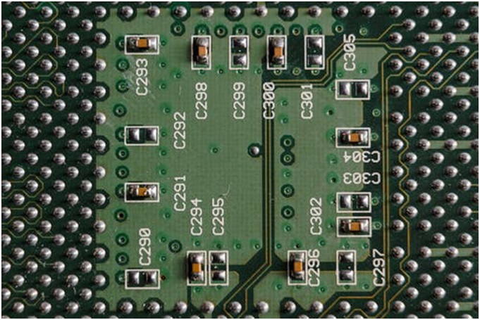
The QFN package is the most popular surface-mount IC package assembled on printed circuit boards to install micro-devices. These tiny packages come in different types and are ideal for automotive, industrial, consumer, and power applications.
What is a QFN Stencil?
The QFN stencil is a thin sheet made of stainless steel that comes in handy to imitate the initial manufacturing process and place a uniform volume of solder paste on the electronic circuit boards. So, if you want to develop smooth QFN packages for your printed circuit boards, you need to buy QFN stencil from a trusted vendor that guarantees precision and robustness at the same time.
What does QFN stand for?
QFN is the short-for Quad Flat No-Lead package available in small sizes and provides moderate heat dissipation in printed circuit boards. Like any other package you might know about, such as BGA or Ball Grid Array, the job of a QFN package is to combine the silicon die of the “Integrated Circuit” with the printed circuit board.
What are the different characteristics of standard QFN packages?
Before you buy a QFN stencil, it is imperative to know some critical properties of the standard QFN packages:
- Their minimum to maximum seated height ranges from 0.35mm to 2.10mm, while the standard one is 0.85mm.
- They are halogen-free and lead-free
- Their terminal plating gets composed of Ni-Pd-Au and Sn
- They comply with RoHS, REACH, and ELV
If you want to know some of the commonly used versions of QFN packages, they are Very Thin QFN (VQFN), Thin QFN (TQFN), and Micro Lead Frame (MLF).
What are the advantages of using QFN packages for your PCBs?
Some of the pros of QFN packages are:
- They are easy to handle and also lightweight.
- They are suitable for applications that need a high amount of heat dissipation.
- They are famous for low inductance between leads.
- They have a small size and comes with a thin profile.
- The short bond wires connect the die and frame.
- The best thing? These QFN packages are available for sale at a low cost.
What are the different types of QFN packages?
The QFN packages are mainly of two types based on the moulding – punch-type and sawn-type.
-
Punch-type
In a punch-type fixture, the QFN package gets moulded in the single mould cavity format, which gets separated with the help of a punch machine. It means that in this method, only a single package gets moulded into a punch-type shape.
-
Sawn-type
To mould sawn-type fixtures, the manufacturers use the Mould Array Process, i.e., also called MAP. In the MAP method, the large set of packages gets cut into various parts. Additionally, a final saw process gets utilized for separating the sawn-type structures into individual ones.
How vital are QFN stencils for your PCB assembly?
Do you know that solder paste deposition on your PCB is an instrumental process that determines your whole electronic assembly’s final quality and performance? And what might shock you is that the solder paste deposition is challenging to perform without using the appropriate stencils. It is the main reason professionals design QFN stencils according to the standard IC requirements.
What’s more, the QFN packages get widely used by electronic item manufacturers because of their excellent electrical and thermal performance. They are generally available in square or rectangular shapes whose package forms are somewhat identical to BGA packages. The primary area where QFN differs from BGA is that the former does not have solder balls at the bottom.
Now you may want to know how does it connect to the circuit board, right? Well, to establish an electrical and mechanical connection with other devices, the solder joints come in handy that get generated through reflow soldering. However, before that, the solder paste needs to get applied on pads that are available on the printed circuit board’s surface.
Summary
We hope you learned a lot of things about QFN packages and stencils in this post today. So, if you want to purchase QFN stencils right away, visit a cutting-edge electronics ecommerce site now.