A Detailed Discussion on PCB Inspection Methods
In the electronics industry, high-quality printed circuit boards (PCBs) have become a prime necessity. These PCBs act as an integral component of different electronics. Therefore, different electronic devices’ smooth operation would be at risk if they fail to operate because of manufacturing errors. To prevent this, PCB manufacturers and assembly providers are currently conducting different PCB inspections at various stages of production. This post addresses the different methods of PCB Inspection System and the types of defects they examine.
Importance of PCB inspection methods
Today, the detection of manufacturing defects is difficult due to the growing sophistication of PCBs. They may also have faults such as holes and shorts, wrong orientation, inconsistencies in soldering, misalignment of components, the incorrect placing of the components, faulty non-electrical and electrical components, missing electrical components, etc. PCB manufacturers use the following inspection methods to prevent any of these variables.
All of the techniques discussed above for PCB Inspection System ensure precise inspection of electronic assemblies and assist PCB assemblers in ensuring their consistency before leaving the facility. It is important to source from trusted PCB assembly providers if you consider PCB assemblies for your next project. Many companies are supplying their customers with PCB assemblies across industries such as aerospace and satellite, industrial electronics products, computer and business electronics, medical, military, wireless, and telecommunications.
Basics for PCB Inspection
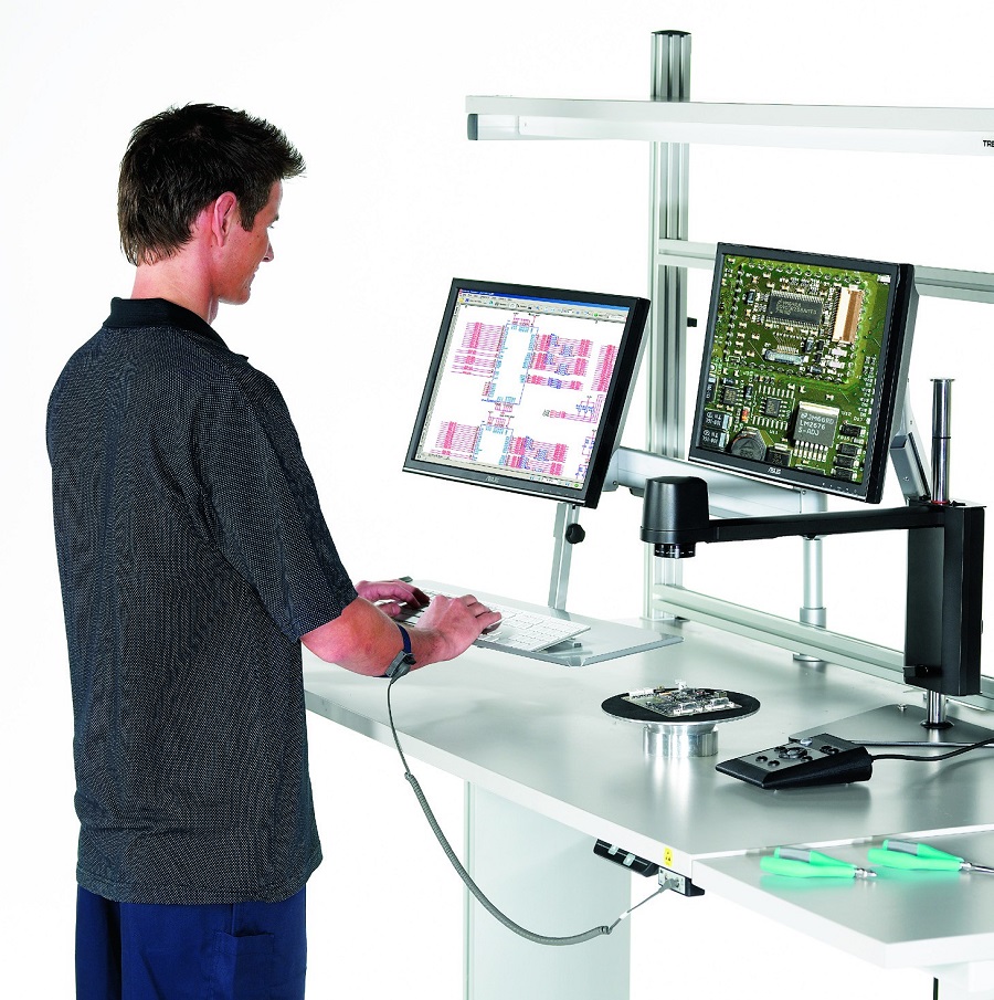
In the early days of PCBs or any electronic equipment, all inspections were carried out manually. The best choice was this, but it was known as having only minimal value. The process’s repetitive nature resulted in several defects not being identified and not recognized in the next step.
There are different techniques by which PCB inspection can be done:
Assembly inspections of printed circuit boards focus mainly on verifying the proper positioning and soldering of PCBs’ electronic components. To do this, the contract manufacturer can use these major inspection processes:
- Automatic solder paste inspection (SPI): SPI systems use a laser scanner and high-resolution image processing for inspecting the form, volume, and alignment of the solder paste pad in the board using the same files for the development of solder app stencils. Depending upon the part to be added, the amount of solder paste on a pad may vary, and the shape of that solder may differ from the pad used to minimize solder voids and bridges. Manual solder paste inspection is inefficient in such a way. However, automated systems will tell the operator if the solder is appropriate on the board or even when soldering equipment needs to be cleaned or changed. Completely effective SPIs are important for small high-density pieces, such as ball grid arrays (BGA), which hide solder joints from automated optical inspection systems.
- First article manual inspection: The inspector shall inspect the entire parts of the material bill (BOM) after connecting the components to the first circuit board until the board undergoes a solder reflow operation. To create the known “golden” board for the automated optical inspection process, the inspector will ensure that the components align with the BOM and that their position and rotation are correct. This board is then passed through the automated optical inspection system to produce a “golden” collection of images automatically compared to the rest of the manufactured boards.
- Automated optical inspection (AOI): The AOI system can compare components for correct placement and all clear solder joints on subsequently manufactured boards using the established “golden” first item board as the reference. To verify component labels, such as polarity indications and resistor color bands, this device utilizes a combination of illumination wavelengths and high-resolution cameras. Open solder joints, inadequate solder, solder bridges, and misaligned pieces can be identified.
Depending on the needs of the boards being processed, the system may also be tuned. False defect warnings may be tuned out, thus rendering those irregularities more vulnerable to alerting the operator to sensitive areas. It is also possible to program the AOI system to consider alternate parts as well.
This method of PCB inspection is frequently used and has been refined so that it performs very reliably.
- AXI PCB inspection: Not all solder joints may be noticeable as density on PCBs increases and new IC mounting technologies are being used. It is essential to check that solder joints on packages such as BGAs (Ball Grid Arrays) are properly soldered, especially when new boards are being manufactured, and new set-ups are being used. This cannot be done by visual inspection since the solder joints are not visible. The only choice is to use the X-Ray system – Automatic X-Ray Inspection, AXI, which allows the solder joints to be viewed under the chips. In certain cases, although costly and only used for a limited proportion of the solder joints, etc., they are required.
Most manufacturers use AOI systems for their PCB Inspection System functions for high volume production these days. AXI is also increasingly used to rise in the number of BGAs and BGA based packages being used.